Brain-inspired Computing based on emerging Non-volatile Memory Devices (III) - Xin Zhang, Ph.D
2021-11-11
1. Why is eNVMs attractive for hardware implementations of neural computing?
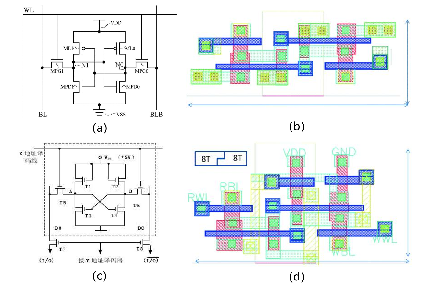
To overcome the challenges faced by synapses based on static random-access memory (SRAM), Researchers propose to utilize the unique characteristics of eNVMs (Emerging nonvolatile Memory) to better serve the simulated synapses in neural networks. The goal is to replace SRAM arrays with resistive cross bar arrays to store and/or update weights in a more parallel manner. With six or eight transistors binary than an SRAM cell (as shown in figure 1, the area is large, store information co., LTD.), smaller eNVM unit takes up the area of more than dozens of times, and each unit can store multiple bits, which further increases the integration density, enabling greater on-chip capacity (for a bigger problem or data set). From a system-wide perspective, reducing or eliminating off-chip memory access by restoring most or ownership on the chip is critical to speed up and reduce power consumption. Due to non-volatility, eNVM devices can also be turned off and on immediately, with no standby leakage. In addition, unlike conventional SRAM arrays that write and read sequentially, resistance cross rod arrays with eNVMs can be programmed in parallel and weighted summation for further acceleration, making online training possible.

Figure 1 schematic diagram and layout of SRAM circuit, (a) schematic diagram of six-tube SRAM; (b) 6-tube SRAM layout; (c) 8-tube SRAM schematic diagram (d) 8-tube SRAM layout
In general, eNVMs are mostly resistive stores that use resistors to represent and store data, while ferroelectric stores use capacitors to represent and store data. Resistance-based eNVMs include self-rotating moment magnetic Random access Memory (STT-MRAM) [1], phase change memory (PCM) [2], and resistive random access memory (RRAM) [3]. RRAM has two subcategories [4] : one is anionic oxide Random access Memory (OxRAM) and the other is cATIONic conductive Bridge Random access Memory (CBRAM) [5]. In some literature, resistive memory is also called a memristor (memristor) [6]. In this paper, we will focus on PCM and RRAM technologies, as they have been shown to have multistage states, and briefly discuss the application of ferroelectric field effect transistors (FeFET) and floating gate transistors (basic units of current flash technology) in synaptic devices. ENVMs is being studied primarily as the next generation of storage-level storage technology with active industrial research and development [7]. For example, Samsung has reported a 20nm node 8Gb PCM prototype chip with 40Mb /s write bandwidth [8]. Sandee/Toshiba has released a prototype 32GB RRAM chip with 24nm nodes [9]. Micron/SONY reported a 27nm node 16Gb CBRAM prototype chip with 200Mb/s write bandwidth and 1Gb/s read bandwidth. Panasonic's commercial microcontroller product has embedded TaOx RRAM with Megabyte capacity [10]. These examples show that eNVMs is a feasible technology for potential large-scale neural network integration.

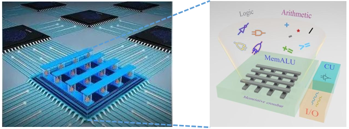
Figure 2. Schematic diagram of cross rod array concept based on eNVM device
2. Device-level characteristics of synaptic devices
2.1 Expected Features
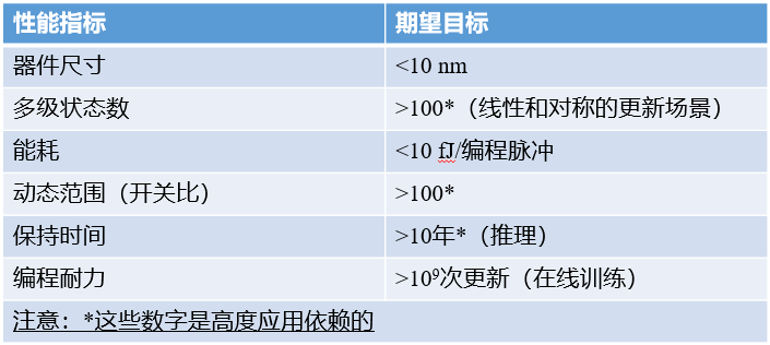
The ideal properties of resistive synaptic devices for improving learning accuracy and energy efficiency are discussed here. Table 1 summarizes the desired performance indicators for resistive synaptic devices. It is worth noting that many of the metrics are highly application dependent (relevant to different scenarios, for example, online or offline training, data set size, etc.).
Table 1 Expected performance indicators of synaptic devices

(1) Device size
Large scale integration of neural networks requires compact and small area synaptic devices. Resistive synaptic devices with sub-10 nm extension characteristics are preferred. Today's RRAM and PCM devices have demonstrated this scalability, but most examples so far have been for digital memory applications. Therefore, the tradeoff between scalability and simulated synaptic features such as multilevel states and dynamic ranges needs to be further characterized. Ultimately, a dual-terminated eNVM device (ideally with a dual-terminated selector) compatible with cross-bar array architecture and 3D integration is the goal of future research.
(2) Multi-level state
The synaptic plasticity observed at biological synapses is characterized by similar behaviors with multiple synaptic weight states. Most neuro-inspired algorithms also use simulated synaptic weights to learn patterns or extract features. In general, more multilevel states (e.g., > hundreds of levels) translate into better learning and better network robustness. However, the weight accuracy requirement (i.e. the number of conductance states) remains strongly dependent on the application scenario. In general, online training requires more state levels than reasoning. If the multilevel states in a resistive synaptic device are insufficient to meet the accuracy requirements of the algorithm, two alternative solutions are available: first, multiple devices can be grouped to represent higher accuracy at the cost of area and energy consumption [11]. Second, recent work has shown that binary synaptic devices with random weight updates can provide analog synaptic properties equivalent to some simple neural networks [12].
(3) Dynamic range
Dynamic range is the on/off ratio between maximum and minimum conductance. Most candidate resistive synaptic devices exhibit a range of 2x to greater than 100x. The larger the dynamic range, the better the ability of the weights in the algorithm to map to the conductance in the device, because the weights in the algorithm are usually normalized over a range (for example, between 0 and 1). For example, an on/off ratio of 100 means that the minimum weight that can be expressed is 0.01. Taking into account the power consumption of parallel reading, the weights in massively integrated neural networks (e.g., matrix size 512 × 512 or above), the guidelines for the range required by A single device can range from 10nS to 1μS to limit the maximum column current to A few hundred μA for practical circuit design.
Reference Catalogue:
[1] J.-G. Zhu, "Magnetoresistive Random Access Memory: Finite Element Modeling and Optimization: The path to scalability and scalability competitiveness, "Proc. IEEE transactions on Industrial Intelligence, Vol. 96, No. 11, pp. 1586 -- 1598, Nov. 2008.
[2] H.-S. P. Wong et al., "Phase Change memory," Proc. IEEE, Vol. 98, No. 12, pp. 2201 -- 2227, Dec. 2010.
[3] H.-S. P. Wong etal., "Metal-oxide RRAM," Proc. IEEE, Vol. 100, No. 6, pp. 1951-1970, Jun. 2012.
[4] A. Graves, A. r. Mohamed, and G. Hinton, "Speech Recognition in Deep Recurrent neural networks," In Proc. IEEE int.conf.acoust. Speech Signal Process. (ICASSP), May 2013, pp. 6645 -- 6649.
[5] ImageNet. [Online]. Available: http://www. image-net.org/
[6] J. J. Yang, D. B. Strukov, and D. R. Stewart, "Memristive Devices for Computing," Nature Nanotechnol., Vol. 8, No. 1, pp. 13 -- 24, 2013.
[7] S. Yu and P. Y. Chen, "Emerging memory Technologies: Recent Trends and Prospects, "IEEE Solid-State Circuits Mag., Vol. 8, No. 2, pp. 43 -- 56, 2016.
[8] Y. Choi et al., "A 20 nm 1.8V 8Gb PRAM with 40 MB/s Program bandwidth," In IEEE Int. Solid-state Circuits Conf. (ISSCC) Dig. Tech. Papers, Feb. 2012, pp. 46 -- 48.
[9] T.-Y. Liu et al., "A 130.7 mm 2 2-layer ReRAM Memory Device in 24nm Technology," In IEEE Int. Solid-state Circuits Conf. (ISSCC) Dig. Tech. Papers, 2013, pp. 31.6.1 -- 31.6.4.
[10] Cross-point ReRAM Macro with a write throughput of 492 MB/s," in IEEE Int. Solid-State Circuits Conf. (ISSCC) Dig. Tech. Papers, 2012.
[11] S. Yu, "Binary Neural Network with 16 Mb RRAM Macro Chip for Classification and Online Training," in IEDM Tech. Dig., Dec. 2016.
[12] S. Yu, B. Gao, Z. Fang, H. Yu, J. Kang, and H.-S. P. Wong, "Stochastic Learning in Oxide binary Synaptic Device for Neuromorphic Computing," Front. Neurosci., vol. 7, p. 186, Oct. 2013.
