Brain-inspired computing based on emerging nonvolatile memory devices - Xin Zhang, PhD
2021-08-03
Brain-inspired Computing based on Emerging Nonvolatile Memory Devices (1)
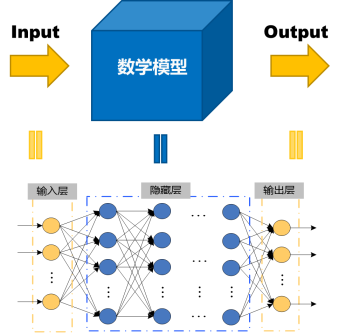
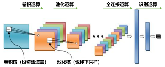
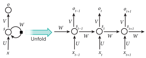
Artificial Intelligence (AI), which enables machines to think and act like humans, is undergoing a Renaissance, and it is not only a hot topic in academia today, but also has significant social implications (for example, the emergence of AlphaGo [1]). In recent years, artificial neural networks (i.e., machine/deep learning) have shown significantly improved accuracy in large-scale visual/auditory recognition and classification tasks, some of which even exceed the human level [2]. Figure 1 shows a basic deep neural network diagram, including an input layer, a hidden layer and an output layer. In particular, Convolutional Neural Network (CNN) [3] and Recurrent NN (RNN) [4] algorithms and their variants have proved their effectiveness in image, video, voice, and biomedical applications. FIG. 2 and FIG. 3 respectively show the schematic diagrams of CNN and RNN. To improve accuracy, the most advanced deep learning algorithms today tend to actively increase the depth and size of the neural network. For example, Microsoft's Res-Net (which won the ImageNet 2015 Image Classification Contest [5]) is over 100 layers deep [6]. This poses significant challenges to hardware implementations in terms of computing, memory, and communication resources. For example, Google's stacked auto-coding algorithm was able to successfully identify cat faces from 10 million random images taken from YouTube videos [7]. However, the task was done on a cluster of 16,000 processor cores, which consumed about 100 kilowatts of power and took three days to train the network.
Xin Zhang - Brain-inspired computing based on emerging non-volatile memory devices (I).png

Figure 1. Schematic diagram of deep neural network operation

FIG. 2 Schematic diagram of convolutional neural network operation

FIG. 3 Structure diagram of cyclic neural network (left) and its expansion form (right)
Today, deep learning is typically trained via a Graphic Processing Unit (GPU) accelerator in a data center or cloud platform. Specially designed accelerators such as SpiNNaker of Manchester [8] (FIG. 4), BrainScaleS of Heidelberger [9] (FIG. 5) and The Tensor Processing Unit of Google, TPU[10] has been developed to run large-scale neuromorphological and/or deep learning algorithms. In embedded systems or computing on the edge of the Internet of Things (IoT), such as autonomous driving, smart sensors, wearables, etc., there are serious design constraints in terms of performance, power, area, etc. In silicon complementary metal oxide semiconductor (CMOS) technology, IBM's TrueNorth[11], MITs Eyeriss[12] and a series of CNN accelerators [13]-[15] have developed application-specific integrated circuit (ASIC) on-chip solutions. However, there are still limitations in terms of on-chip memory capacity, off-chip memory access, and online learning capabilities. In particular, CMOS ASIC designs show that on-chip storage is the biggest bottleneck of energy efficiency computing, that is, storing millions of parameters and loading them from off-chip main memory to on-chip cache requires a large amount of energy and latency. Today's CMOS ASIC accelerators typically utilize static random access memory (SRAM) as the on-chip synaptic memory. Although SRAM technology has kept up well with CMOS scaling trends, the density of SRAM (100~200F2 per bit unit; Where F represents the technology node) and on-chip SRAM capacity (usually a few megabytes) are insufficient to store a large number of parameters (usually several hundred megabytes) in deep learning algorithms. The line-by-line operation of a traditional SRAM array limits the parallelism of the system, and leakage current is not desirable.
As an alternative hardware platform, emerging Nonvolatile Memory (eNVM) is proposed for on-chip weight storage with higher density (usually 4~12F2 per bit unit) and fast parallel simulation with low leakage power [16]. A special subset of eNVM devices that can display multistage resistance/conductance states can naturally simulate synaptic devices in neural networks, namely resistive synaptic devices [17]. Examples of Resistive synaptic devices include double-ended eNVMs, such as Phase Change Memory (PCM), Resistive Random Access Memory (RRAM), And a three-terminal ferroelectric transistor and a floating gate memory (with analog threshold voltage). The parallelism of the resistance cross bar array matrix vector multiplication (or dot product) further significantly accelerates the core neural computation (i.e., the weighted summation). A recent analysis by IBM showed that PCM based accelerators can train fully connected Multilayer Perceptron (MLP) at a lower power consumption than traditional Gpus [18]. By optimizing device technical parameters, it is possible that the ACCELERATOR based on eNVM is superior to the accelerator based on CMOS-ASIC SRAM synaptic array [19].
In the past few years, significant progress has been made in the research of enVM-based synaptic devices and their integration into the array level. At the device level, many candidates for resistive synaptic devices with tens to hundreds of conductance states have been demonstrated. Resistive synaptic devices can mimic biological synapses, where the migration/rearrangement of ions or atoms in solid media (e.g. oxides/chthiocompounds) can regulate the conductance between two electrodes, similar to how biological synapses regulate their conductance through the activation of volt-gated calcium channels. At the array level, there have been some experimental demonstrations of simple neural network algorithms using software and/or off-chip controllers from small scale (e.g. 12 × 12) to medium scale (e.g. 256 × 256). These demonstrations show great promise for future large-scale integration and prototyping of on-chip CMOS controllers. In addition, the development of computer-aided Design (CAD) or Electronic Design Automation (EDA) tools has facilitated the joint optimization of device performance with circuit/architecture and algorithm as the array size expands. To address design challenges related to device yield, device variability, and array parasitism. Groundbreaking simulation frameworks have been developed to evaluate the impact of device-level nonideality (finite weight accuracy, weight update nonlinearity/asymmetry, variation/noise, etc.) on the tradeoff between learning accuracy and training speed/energy.
Reference directory:
[1]D. Silver et al., “Mastering the game of go with deep neural networks and tree search,” Nature, vol. 529, pp. 484–489, 2016.
[2]Y. LeCun, Y. Bengio, and G. Hinton, “Deep learning,” Nature, vol. 521, pp. 436–444, May 2015.
[3]A. Krizhevsky, I. Sutskever, and G. E. Hinton, “ImageNet classification with deep convolutional neural networks,” in Proc. Adv. Neural Inf. Process. Syst. (NIPS), 2012, pp. 1097–1105.
[4]A. Graves, A.-R. Mohamed, and G. Hinton, “Speech recognition with deep recurrent neural networks,” in Proc. IEEE Int. Conf. Acoust. Speech Signal Process. (ICASSP), May 2013, pp. 6645–6649.
[5]ImageNet. [Online]. Available: http://www. image-net.org/
[6]K. He, X. Zhang, S. Ren, and J. Sun, “Deep residual learning for image recognition,” in Proc. IEEE Conf. Comput. Vis. Pattern Recognit. (CVPR), Jun. 2016, pp. 770–778.
[7]Q. V. Le, “Building high-level features using large scale unsupervised learning,” in Proc. Int. Conf. Mach. Learn. (ICML), 2012, pp. 8595–8598.
[8]S. B. Furber, F. Galluppi, S. Temple, and L. A. Plana, “The SpiNNaker project,” Proc. IEEE, vol. 102, no. 5, pp. 652–665, May 2014.
[9]S. Schmitt et al., “Neuromorphic hardware in the loop: Training a deep spiking network on the BrainScaleS wafer-scale,” in Proc. Int. Joint Conf. Neural Netw. (IJCNN), 2017.
[10]N. P. Jouppi et al., “In-datacenter performance analysis of a tensor processing unit,” in Proc. ACM/IEEE Int. Symp. Comput. Architecture (ISCA), 2017.
[11]P. A. Merolla, “A million spiking-neuron integrated circuit with a scalable communication network and interface,” Science, vol. 345, no. 6197, pp. 668–673, Aug. 2014.
[12]Y.-H. Chen, T. Krishna, J. Emer, and V. Sze, “Eyeriss: An energy-efficient reconfigurable accelerator for deep convolutional neural networks,” in IEEE Int. Solid-State Circuits Conf. (ISSCC) Dig. Tech. Papers, Feb. 2016, pp. 262–263.
[13]J. Sim, J.-S. Park, M. Kim, D. Bae, Y. Choi, and L.-S. Kim, “A 1.42 TOPS/W deep convolutional neural network recognition processor for intelligent IoE systems,” in IEEE Int. Solid-State Circuits Conf. (ISSCC) Dig. Tech. Papers, Jan. 2016, pp. 264–265.
[14]G. Desoli, “A 2.9 TOPS/W deep convolutional neural network SoC in FD-SOI 28nm for intelligent embedded systems,” in IEEE Int. Solid-State Circuits Conf. (ISSCC) Dig. Tech. Papers, Feb. 2017, pp. 238–239.
[15]B. Moons, R. Uytterhoeven, W. Dehaene, and M. Verhelst, “ENVISION: A 0.26-to-10TOPS/W subword-parallel dynamic-voltage-accuracy-frequencyscalable convolutional neural network processor in 28 nm FDSOI,” in IEEE Int. Solid-State Circuits Conf. (ISSCC) Dig. Tech. Papers, Feb. 2017, pp. 246–247.
[16]S. Yu, Ed., Neuro-Inspired Computing Using Resistive Synaptic Devices. New York, NY, USA: Springer-Verlag, 2017.
[17]D. Kuzum, S. Yu, and H.-S. P. Wong, “Synaptic electronics: Materials, devices and applications,” Nanotechnology, vol. 24, no. 38, p. 382001, 2013.
[18]G. W. Burr et al., “Large-scale neural networks implemented with non-volatile memory as the synaptic weight element: Comparative performance analysis (accuracy, speed, and power),” in IEDM Tech. Dig., 2015.
[19]B. Rajendran et al., “Specifications of nanoscale devices and circuits for neuromorphic computational systems,” IEEE Trans. Electron Devices, vol. 60, no. 1, pp. 246–253, Jan. 2013.
